1. Limitations of near-infrared wavelength high power lasers
In recent decades, high-power continuous wave (CW) lasers have become a ubiquitous tool in modern manufacturing industries. These lasers are used for a wide range of applications, including welding, cladding, surface treatment, hardening, brazing, cutting, 3D printing, and additive manufacturing.
The first significant development in high-power CW laser technology occurred before the year 2000, with the creation of the high-power 10.6 µm wavelength carbon dioxide (CO2) laser and the near-infrared 1064nm wavelength semiconductor-pumped Nd:YAG solid-state laser.
However, due to its wavelength, the carbon dioxide laser is difficult to transmit through optical fibers, making it challenging for industrial applications. Similarly, solid-state lasers are limited by brightness and power amplification.
After 2000, high-power industrial fiber lasers were developed as a solution that can be transmitted through optical fibers while still having high brightness and power. Nowadays, fiber lasers have replaced carbon dioxide lasers in most applications and have proven highly effective in many industrial processing applications. In recent years, fiber lasers have become the primary industrial laser used for processes like laser welding and cutting, as they offer higher speed, efficiency, and reliability than carbon dioxide lasers.
However, these continuous high-power fiber lasers generally operate at near-infrared (NIR) wavelengths of less than 1µm. While this is suitable for many applications, some metals will reflect 90% or more of the near-infrared laser radiation that’s incident on their surface, limiting their effectiveness. Yellow metals, such as copper and gold, are particularly challenging to weld with near-infrared lasers due to their low absorption rates, which requires a large amount of laser power to start the welding process.
There are two main laser welding processes: heat conduction mode welding, which involves melting and solidifying the material, and deep penetration welding, which vaporizes the metal and forms a cavity or keyhole.
Deep penetration welding requires a highly absorbed laser beam, as the laser interacts with metal and metal vapor multiple times when propagating through the material.
Starting a keyhole with a near-infrared laser requires a high incident laser intensity, especially when the material being welded has high reflectivity. Once the keyhole is formed, however, the absorption rate increases sharply.
High-power near-infrared lasers generate a high metal vapor pressure in the molten pool, leading to spatter and pores. Thus, laser power or welding speed must be carefully controlled to prevent excessive spatter.
When the molten pool solidifies, “bubbles” in the metal vapor and process gas can be trapped, forming pores in the welding joint. These pores weaken the welding strength and increase joint resistivity, lowering the quality of the welded joint.
Processing materials with an absorptivity of less than 5% at 1µm, such as copper, with near-infrared lasers is a significant challenge. Methods such as generating plasma on processed materials can increase the laser absorptivity of the materials. However, these methods limit material processing to the deep penetration process and carry inherent risks such as sputtering and controlling energy deposition.
Therefore, existing 1µm wavelength laser systems have limitations in processing high-reflective materials like non-ferrous metals and underwater applications.
Related reading: Ferrous vs Non-ferrous Metals
To advance near-infrared laser applications, researchers must investigate new laser sources. Additionally, the shift towards electric engines in new energy vehicles as a means of reducing greenhouse gases has resulted in a significant demand for reliable copper processing solutions. Electric engines, particularly power batteries, require large amounts of copper materials. This demand extends to other renewable energy systems, including wind turbines.
2. The birth of high power blue laser
The development of industrial laser technology has followed the roadmap of production technology and social demands. Over the past 60 years, laser technology has contributed significantly to solving important future tasks, such as the digital economy, sustainable energy, and healthy living.
Today, laser technology has become an indispensable component in several core areas of China’s economy, including production technology, automotive engineering, medical technology, measurement, environmental technology, and information and communication technology. As metal processing technology continues to progress, and user requirements continue to improve, lasers must innovate in cost, energy efficiency, and laser system performance.
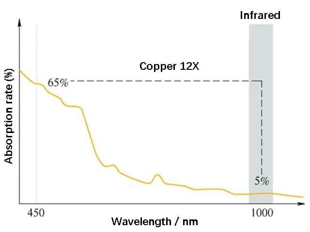
The market demand for effective processing of highly reflective metals has stimulated the development of blue high-power laser technology, which will undoubtedly open doors to new metal processing technologies. In non-ferrous metals, light energy absorption increases as light wavelength decreases. For example, copper’s light absorption at wavelengths below 500nm increases by at least 50% compared to infrared light, making shorter wavelengths more suitable for copper processing.
However, developing short-wavelength, high-power lasers for industrial applications is challenging due to the limited options available. Even the existing options are expensive and inefficient. For instance, there are frequency-doubling-based solid-state laser sources on the market that can produce 515nm and 532nm (green spectrum) lasers in this wavelength range, but these sources rely on nonlinear optical crystals to convert pump laser energy into the target wavelength energy, resulting in high power loss.
Moreover, such lasers require complex cooling systems and intricate optical settings.
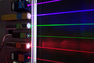
To meet this challenge, attention has turned to blue semiconductor lasers. Blue light has unique properties that make it advantageous for metal processing of high reflection materials like copper. Fig. 1 shows that copper absorbs blue light 13% more efficiently than infrared light, even up to 13 times greater absorption.
Moreover, blue light absorption by copper remains consistent even as the metal melts, providing a stable energy density for welding. As a result, blue laser welding offers precise control, few defects, and produces high-quality copper welds quickly.
Blue light also has long transmission ranges in seawater because it is less absorbed, making it suitable for exploring underwater laser material processing.
Furthermore, blue light is relatively easy to convert to white light, enabling the compact use of blue lasers for floodlights and other lighting applications.
Semiconductor lasers based on gallium nitride can directly produce a laser with a 450nm wavelength, without the need for further frequency doubling, thus achieving higher energy conversion efficiency.
Source: NASA 1969
a) The performance advantages of blue laser stem from the basic physical principles
| Key metals | Blue light absorption |
| Gold | 66X |
| Copper | 13X |
| Aluminum 1100 | 3X |
| Nickel | 1.5X |
b) Comparison of blue light absorption and infrared (NIR) absorption of copper
Fig. 1 Physical properties of blue light
The 450 nm laser is expected to have a processing efficiency nearly 20 times higher than that of the 1 µm laser. When compared to the traditional near-infrared laser welding process, the high-power blue laser offers both quantitative and qualitative advantages.
In terms of quantitative advantages, the blue laser improves welding speed, expands the process range, increases production efficiency, and reduces production downtime.
Regarding qualitative advantages, the blue laser enables a larger process range, produces high-quality welds without splashes or porosity, provides higher mechanical strength, and reduces resistivity. The consistency of welding quality greatly improves production yield (refer to Fig. 2).
Moreover, the blue laser can also perform thermal conduction welding mode, which is impossible for the near-infrared laser (refer to Fig. 3).
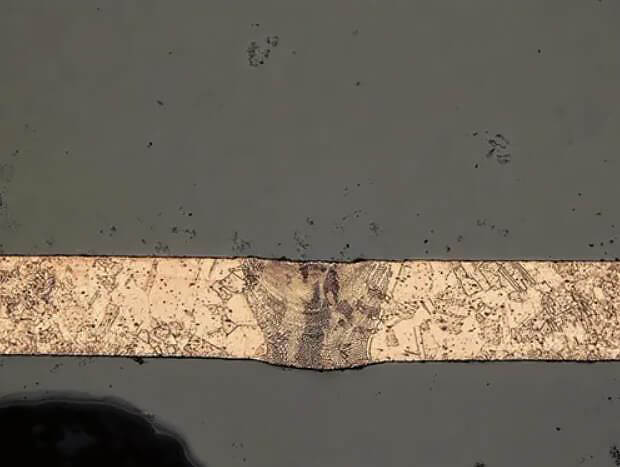
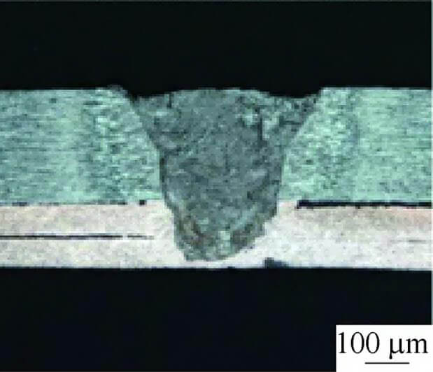
Fig. 2 Cross-section of deep penetration welding on 254 µ m thick copper foil
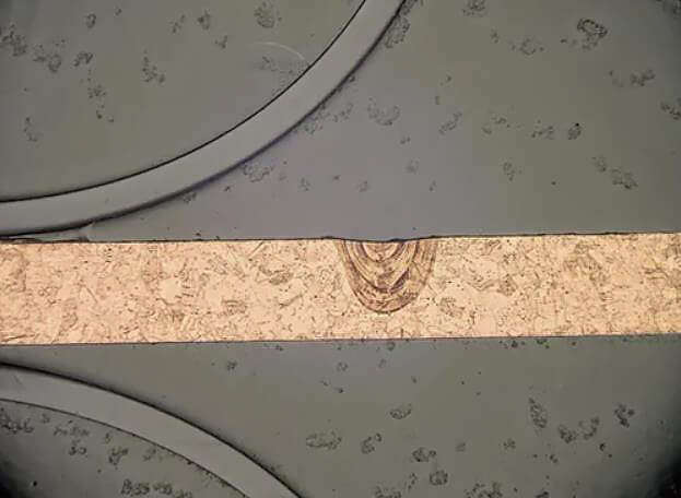
Fig. 3 Section of heat conduction welding mode in copper sheet with a thickness of 500 µm
3. Development of high power blue laser
Gallium nitride (GaN) light-emitting devices have gained significant attention, particularly in the field of lighting, due to the 2014 Nobel Prize in Physics and the increasing global awareness of environmental protection.
With the continuous improvement of high brightness and output of blue semiconductor devices, blue semiconductor lasers have entered the era of mass production. They are commonly used as projector light sources and, in combination with phosphors that produce green or red light, are replacing lamps in projectors.
In recent years, blue semiconductor lasers have gained popularity in lighting and display applications due to their longer life and smaller size compared to bulbs. However, for laser processing, higher power than these blue lasers is necessary.
Despite the advantages of blue lasers, which include longer life and smaller size, developing high-power blue lasers for laser processing requires higher power output than a single blue laser semiconductor chip, which has only a few watts of output power. Increasing the power to a higher range is a time-consuming and expensive process.
To meet the high power requirements for blue lasers, new technical methods are needed. Currently, the actual power of each chip of blue semiconductor laser is about 5W at a single wavelength. Therefore, beam combination technology is essential to obtain higher power output, which can be achieved by combining the outputs of multiple chips.
Beam combination methods are divided into two types: coherent and incoherent methods. The incoherent method is more practical, as it does not require fine phase control between lasers.
The incoherent method includes several techniques for combining multiple laser beams, such as the spatial combination method which combines multiple beams in space, the polarization combination method which combines orthogonal polarized light using a polarization beam splitter, and the wavelength combination method which combines different wavelengths on coaxial.
Each technique has its own advantages and disadvantages and can be used in combination.
The spatial combination method is particularly suitable for combining multiple laser chips with the same wavelength to achieve high power output.
So far, two high-power synthesis methods have been most successful. Here’s a brief introduction to them:
The first method uses laser bars technology to systematically generate a single laser emitter on a wafer of indium gallium nitride (InGaN).
Initially, individual laser chips are integrated efficiently into a “laser bar”, and each laser bar can produce at least 50W of blue light.
Then, multiple semiconductor laser bars are installed and combined into a semiconductor laser stack through appropriate electrical connections, cooling and heat dissipation, and the use of special optical devices.
The entire semiconductor laser can be combined with one or more semiconductor laser stacks, as shown in Figure 4.
Currently, the laser bar technology can generate up to 2kW of blue light power.
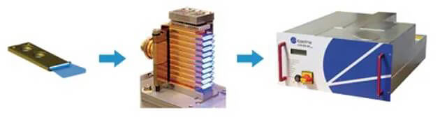
a) Synthesis process of bar instrument
b) Bar beam diagram
Fig. 4 beam synthesis of semiconductor laser bars Technology
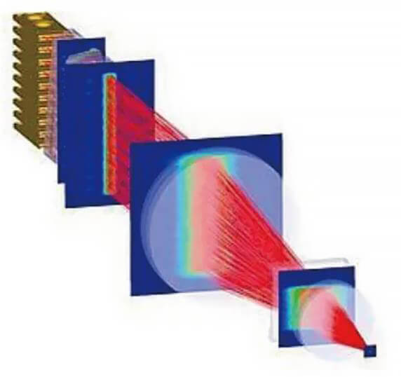
The second method involves the use of semiconductor laser single emitter technology. These lasers utilize a unique “single tube chip based” design that is intended to collimate the output of each gallium nitride (GAN) laser single tube.
If all laser single tubes are collimated together with a single lens, as in the bar technique, the combined beam divergence (BPP) will inevitably increase. However, by collimating each laser single tube with its own special lens, the divergence of the combined beam can be kept as unchanged as possible, and the beam BPP can be minimized, which improves the brightness of the laser (refer to Fig. 5).
Furthermore, as the gallium nitride laser single tube continues to improve in single tube laser power along its expected development path, this unique “single tube chip” design provides the best way to improve the power of the overall laser system.
In addition, laser single tube technology offers the best beam quality with an output power of 1.5KW, providing a guarantee for laser remote processing of galvanometer scanning. This scanning system is widely used in the production of batteries, electric vehicles, and consumer electronics.
During the scanning operation, the laser output power and residence time can be adjusted to maximize productivity by enabling different joint geometry and material thickness to be solved in a single scanning pattern.
Table 1 illustrates the advantages of blue semiconductor laser compared to near-infrared semiconductor laser and green solid-state laser.
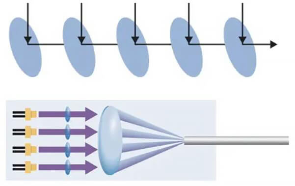
Fig. 5 Beam synthesis of semiconductor laser single tube technology
Table 1 Comparison of blue semiconductor laser with near-infrared semiconductor laser and green solid-state laser
| Project | Blue semiconductor laser | Near infrared semiconductor laser | Green solid state laser |
| Wavelength | Blu ray | Near infrared | Green light |
| Metal absorption | good | commonly | preferably |
| Brightness | good | commonly | good |
| Anti reflection ability | strong | commonly | weak |
| Service life / h | >10000 | >10000 | >5000 |
| Fault type | Service wear | random | random |
| Ease of use and operation | good | good | commonly |
4. Application cases of blue light semiconductor laser material processing
1) Figure 6 illustrates a scanning system consisting of a blue semiconductor laser, used for power battery manufacturing. The advantage of using a blue laser lies in its wide process window, which allows it to handle each stage of battery manufacturing.
Additionally, it can weld thicker materials, such as copper, gold, and stainless steel, that are a few millimeters in thickness. This makes it an ideal choice for manufacturing prismatic batteries, battery housings, and battery packs with integrated batteries.

a) 70 pcs of 8 µm foils welded to 254 µm copper lugs

b) Connection of two copper lugs
c) Connect two copper lugs to the steel battery housing
Fig. 6 the wide process window of the blue laser can handle each stage of battery manufacturing
2) Using a blue semiconductor light source with a 450 nm wavelength, it is possible to melt copper material in the heat conduction mode, allowing for accurate adjustment of the molten pool geometry of thin copper materials (see Fig. 7).
In deep penetration welding of thin copper materials, stable energy absorption and precise control of the heat conduction process are especially important, as they help prevent cutting or splashing of the materials due to high pressure.
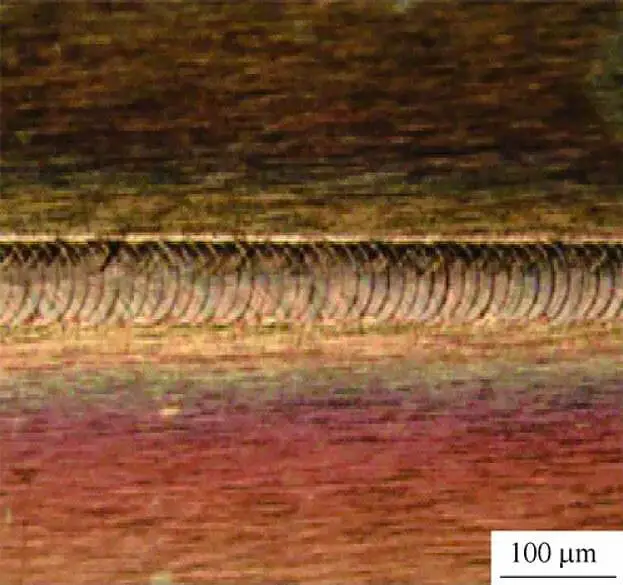
These occurrences are more likely when welding stacked thin copper foils, which can result in irregular gaps due to the warpage of the stacked foils (see Fig. 8).
When butt welding is performed on 34 stacked copper foils with a 580W blue light semiconductor laser at a speed of 2m/min, a weld width of >0.8mm can be formed with minimum porosity and low undercut.
In fillet welding on the edge of the foil stack, the end of the foil can be successfully melted into a high cross-sectional area and completely attached to the solid foil. Perfect mechanical connection and excellent conductivity can be achieved in butt welding and edge welding.
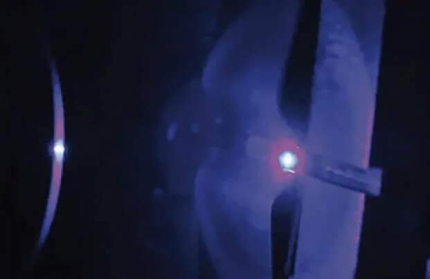
Fig. 7 Molten pool geometry of copper material
a) Edge welding structure

b) At 580W blue laser power and 2m / min welding speed
Fig. 8 joint cross section between 34 stacked copper foils (11 µ m thick each) connection welds
3) Figure 9 illustrates the outcomes of lap welding 30μm-thick copper foils using a 100W blue laser. The welding process involved scanning the top surface of three stacked copper foils at a speed of approximately 10mm/s with the laser.
The laser spot diameter on the sample surface was 100μm due to the concentration of the 100μm core diameter optical fiber output at a projection ratio of 1:1. This resulted in excellent welding quality while minimizing the impact of heat on the surrounding environment and debris.
a) Top view of weld seam
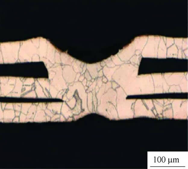
b) Weld seam cross section
Fig. 9 results of lap welding of pure copper sheet
4) Figure 10 depicts an example of a 3D printer made entirely of pure copper, utilizing a blue light semiconductor laser developed by Osaka University. The laser has a focusing spot diameter of 100μm, which enables the lamination of pure copper with high thermal and electrical conductivity on the powder bed. This was previously difficult to achieve with near-infrared lasers.
It is anticipated that this technology will have a wide range of applications in industrial fields, including aerospace and electric vehicles.

a) SLM machine with 100W blue laser
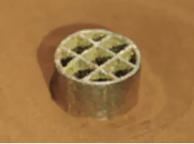
b) 3D prototype sample made of pure copper powder
Fig. 10 3D printing application
5) Greater penetration has also opened up the field of electric vehicle applications, with electric vehicle manufacturers turning to rod winding design to maximize thermal and electrical efficiency. As shown in Figure 11, the consistent quality of the three blue laser hairpin welds is crucial for improving production efficiency.
The blue laser’s ability to produce hairpin welding is particularly important for high-density and high-intensity motor manufacturing.
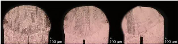
Fig. 11 Application in electric vehicle manufacturing
6) High power and high brightness can increase the flexibility of the welding process, expanding the range of materials that can be processed. For instance, brass, which consists of copper and zinc with significantly different thermal properties, can be challenging to weld with high quality. However, blue industrial laser technology can easily handle this task, allowing for the welding of brass materials commonly used in household appliance production, as shown in Fig. 12.
Preliminary research suggests that blue laser technology can effectively solve the challenge of welding dissimilar metals. Welding dissimilar metals is difficult because each material has unique thermal, optical, and mechanical properties. When dissimilar metals are welded, it can lead to the formation of intermetallic compounds, which are areas of different alloys that damage the mechanical and electrical properties and consistency of the joint.
The latest generation of blue semiconductor lasers has a broad range of process parameters, enabling the welding of different materials with minimal defects. Although copper and zinc in brass have different thermal properties, making high-quality welding difficult, blue semiconductor laser technology can easily handle this challenge.

Fig. 12 Application in brass welding
5. Conclusion
The 2KW blue semiconductor laser has demonstrated its superiority in metal processing, particularly for high reflection metal materials.
The brightness and power of blue semiconductor lasers continue to increase, opening up new possibilities and applications. For instance, the additive manufacturing potential of blue lasers is still being explored (refer to Figure 10).
Moreover, besides efficient metal material processing, blue light semiconductor lasers are expected to be employed in cross-sectoral applications, especially in the mechanical engineering department, enabling the laser processing of materials with blue light underwater.
This advantage is significant for the manufacturing industry. Additionally, the lighting industry can leverage high-quality lighting technology based on blue semiconductor laser.
The emergence of the Internet of Things and Artificial Intelligence is leading to new paradigm shifts in the industrial sector.
Laser processing technology naturally integrates numerical control technology and remote processing, eliminating the need for tool replacement, and will take a leading role in next-generation intelligent manufacturing.
The rise of high-power blue semiconductor laser has also brought a new surprise to laser technology. While processing applications based on high-power blue semiconductor laser are still in their infancy, with future technological advancements, it may become one of the core tools for the next generation of cutting-edge intelligent manufacturing.