Just as manufacturing technology plays a crucial role in various fields today, nanofabrication technology holds a key position in the realms of nanotechnology. Nanofabrication technology encompasses numerous methods including mechanical processing, chemical etching, energy beam machining, and electric field engineering on aluminum surfaces using scanning tunneling microscopy (STM).
There isn’t a unified definition for nanofabrication technology yet; generally, the processing of materials with dimensions below 100nm is referred to as nanofabrication, as is processing with surface roughness at the nanometer level. Nanofabrication refers to part processing where the size accuracy, shape accuracy, and surface roughness are all at the nanometer level.
The following machining technologies can achieve nanoscale processing:
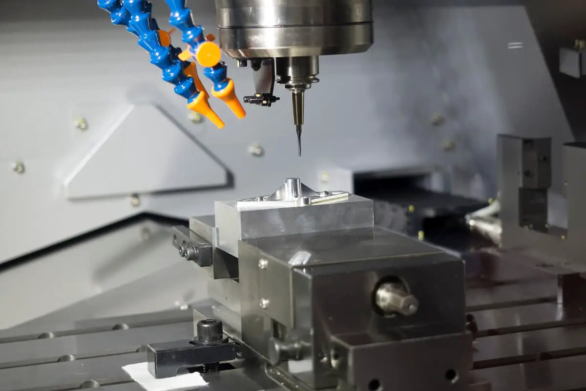
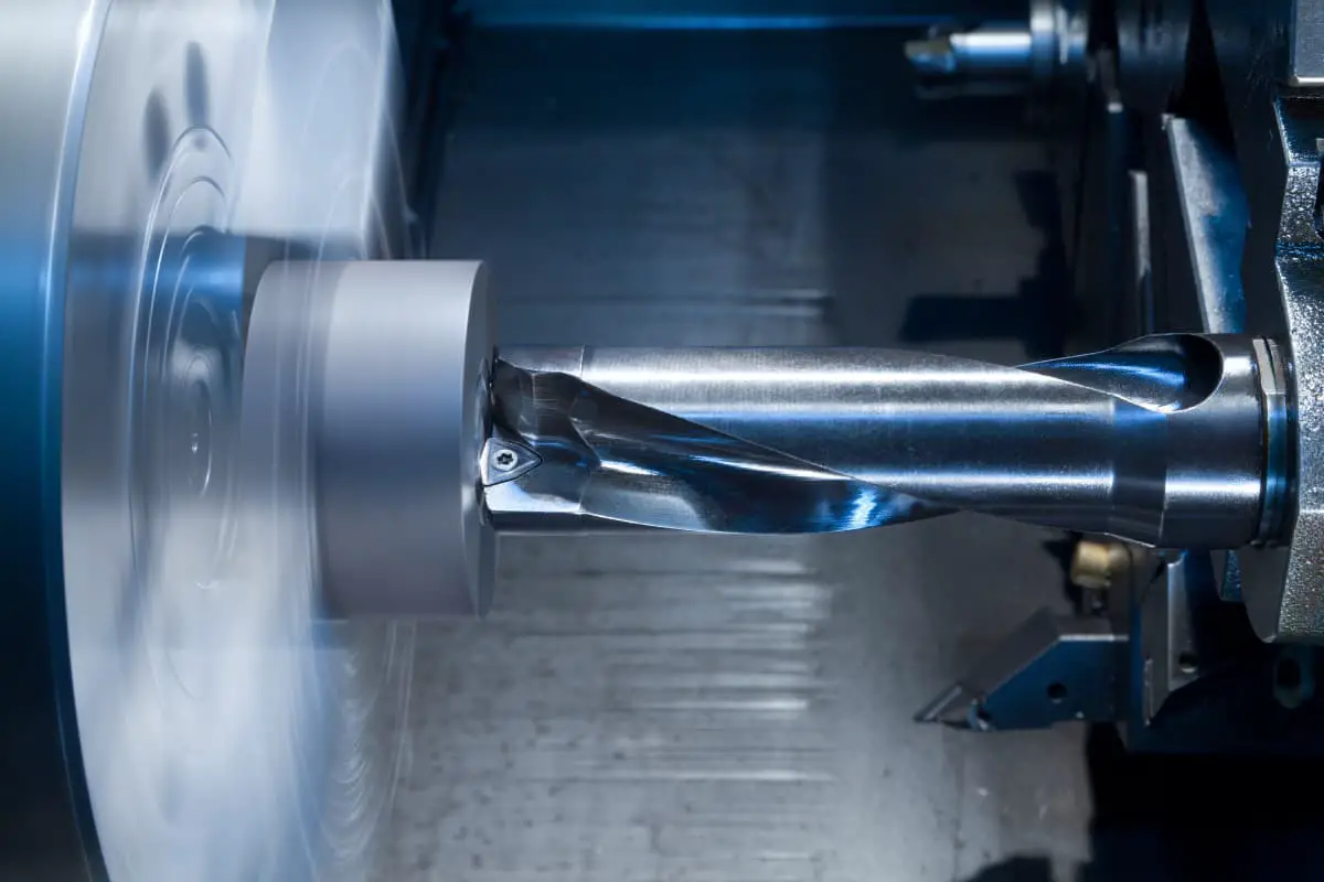
Nanoscale Mechanical Processing Technology
Nanoscale mechanical processing methods include ultra-precision cutting with single-point tools made of single-crystal diamond and CBN, ultra-precision multipoint abrasive processing with grinding tools made of diamond and CBN abrasives, and free abrasive processing or mechanical-chemical composite processing such as grinding, polishing, and elastic emission machining.
Currently, ultra-precision cutting with single-point diamond tools has produced chips as thin as 3nm in labs, and nanoscale grinding has been achieved using ductile grinding technology. Sub-nanoscale removal can be achieved through processes such as elastic emission machining, resulting in surface roughness at the Angstrom level.
Energy Beam Processing Technology
Energy beam processing is a special machining method that uses high-density energy beams, such as laser beams, electron beams, or ion beams, to remove workpiece materials. It mainly includes ion beam processing, electron beam processing, and light beam processing.
Electrolytic jet machining, electrical discharge machining, electrochemical machining, molecular beam epitaxy, and physical and chemical vapor deposition also fall under energy beam processing. Sputtering removal, precipitation, and surface treatment with ion beam processing, as well as ion beam-assisted etching, are also research and development directions for nanoscale machining.
Compared with solid tool cutting, the position and machining rate of ion beam machining are difficult to determine. To achieve nanoscale machining accuracy, a sub-nanoscale detection system and a closed-loop adjustment system for the machining position are needed.
Electron beam machining removes atoms from the surface of the penetration layer in the form of thermal energy, which can be used for etching, photolithography exposure, welding, micromachining, and nanoscale drilling and milling.
In early 1999, deep ultraviolet (DUV) lithography machines for 0.18μm processes had been launched successively. The so-called next-generation lithography (NGL) technologies used to replace optical lithography after 0.1μm mainly include extreme ultraviolet, X-ray, electron beam, and ion beam lithography. A brief introduction to the progress of various lithography technologies is given below.
1. Optical Lithography
Optical lithography projects the structural diagrams of large-scale integrated circuit devices on the mask onto a silicon wafer coated with photoresist through an optical system. The minimum feature size that optical lithography can achieve is directly related to the resolution that the optical lithography system can achieve, and reducing the wavelength of the light source is the most effective way to improve the resolution.
Therefore, the development of new short-wavelength light source lithography machines has always been a hot research topic internationally.
Currently, the wavelength of the light source of commercial lithography machines has moved from the ultraviolet band of mercury lamp light sources in the past to the deep ultraviolet band (DUV), such as the KrF excimer laser (wavelength 248nm) used for 0.25μm technology and the ArF excimer laser (wavelength 193nm) used for 0.18μm technology.
In addition, using the interference characteristics of light and optimizing process parameters with various wavefront technologies is also an important way to improve lithography resolution. These technologies are breakthroughs made by deep analysis of exposure imaging based on electromagnetic theory and lithography practice, including phase-shifting masks, off-axis illumination technology, and proximity effect correction.
Using these technologies, higher resolution lithographic patterns can be achieved at the current level of technology. For example, in early 1999, Canon launched the FPA-1000ASI scanning stepper, which uses a 193nm ArF light source.
With wavefront technology, it can achieve a lithographic linewidth of 0.13μm on a 300mm silicon wafer. Optical lithography technology includes lithography machines, masks, photoresists, and a series of technologies, involving optics, mechanics, electricity, physics, chemistry, materials, and other research fields.
Currently, scientists are exploring F2 laser (wavelength 157nm) lithography with a shorter wavelength. Due to the high level of light absorption, obtaining new optical and mask substrate materials for lithography systems is the main difficulty of this wavelength technology.
2. Extreme Ultraviolet Lithography
Extreme Ultraviolet Lithography (EUVL) employs extreme ultraviolet light with a wavelength of 10-14nm as the light source. Although initially referred to as soft X-ray lithography, it is more akin to optical lithography. The difference is that due to strong absorption in the material, its optical system must be in reflective form.
3. X-ray Lithography
X-ray Lithography (XRL) features a light source wavelength of approximately 1nm. Since it provides high-resolution exposure, XRL has been widely recognized since its invention in the 1970s. Countries with synchrotron radiation devices, such as those in Europe, the United States, Japan, and China, have successively conducted related research.
XRL is the most mature among all next-generation lithography technologies. The main difficulty of XRL lies in obtaining a mask substrate with good mechanical and physical properties. In recent years, significant progress has been made in mask technology. Silicon carbide (SiC) is the most suitable substrate material.
Although XRL is no longer the only candidate for future technologies due to the in-depth research on XRL-related issues, the development of optical lithography, and new breakthroughs in other lithography technologies, the United States has recently reduced its investment in XRL. Nevertheless, XRL remains one of the indispensable candidate technologies.
4. Electron Beam Lithography
Electron Beam Lithography (EBL) uses a high-energy electron beam to expose the photoresist to obtain structural graphics. With its de Broglie wavelength around 0.004nm, EBL is not affected by diffraction limits, achieving near-atomic scale resolution. EBL can achieve extremely high resolution and directly generate graphics.
It is not only an indispensable mask preparation tool in the production of very-large-scale integrated circuits (VLSI) but also the primary method for processing devices and structures for special purposes. The resolution of current electron beam exposure machines has reached below 0.1µm. The main disadvantage of EBL is its low productivity, only 5-10 wafers per hour, far less than the current optical lithography level of 50-100 wafers per hour.
The SCALPEL technology developed by Lucent Technologies in the United States is noteworthy. This technology shrinks mask graphics like optical lithography and uses special filtering techniques to remove scattered electrons generated by mask absorbers, thereby improving output efficiency while ensuring resolution.
It should be noted that regardless of the lithography technology used in the future, EBL will be an indispensable infrastructure for integrated circuit research and production.
5. Ion Beam Lithography
Ion Beam Lithography (IBL) uses ions formed by ionizing liquid or solid-state atoms, accelerated and focused or collimated by an electromagnetic field, to expose the photoresist. The principle is similar to EBL, but the de Broglie wavelength is shorter (less than 0.0001nm), and it has advantages such as a small proximity effect and a large exposure field. IBL mainly includes Focused Ion Beam Lithography (FIBL) and Ion Projection Lithography (IPL).
FIBL was developed earliest, and recent experimental research has achieved a resolution of 10nm. Because of its low efficiency, it is difficult to apply as an exposure tool in production and is currently mainly used as a mask repair tool and special device trimming in VLSI. To address the shortcomings of FIBL, people have developed IPL technology with higher exposure efficiency, and considerable progress has been made.
Lithography Galvanoformung Abformung Technology
Lithography Galvanoformung Abformung (LIGA) process is a comprehensive technology composed of deep synchrotron radiation X-ray lithography, electroforming, and plastic molding. The most basic and core process is deep synchrotron radiation lithography, while electroforming and plastic molding are key to the practical application of LIGA products.
Compared with traditional semiconductor processes, LIGA technology has many unique advantages, such as a wide range of materials that can be used, including metals and their alloys, ceramics, polymers, and glass; it can produce three-dimensional microstructures with a height of several hundred micrometers to one millimeter and aspect ratios greater than 200; lateral dimensions can be as small as 0.5μm, and machining accuracy can reach 0.1μm; it can realize mass replication and production at low cost.
Various micro-devices and micro-devices can be produced with LIGA technology. Successful or ongoing LIGA products include micro-sensors, micro-motors, micromechanical parts, integrated optics and micro-optical components, microwave components, vacuum electronic components, miniature medical instruments, nanotechnology components and systems, etc.
The application of LIGA products covers a wide range, such as machining technology, measurement technology, automation technology, automotive and transportation technology, power and energy technology, aviation and aerospace technology, textile technology, precision engineering and optics, microelectronics, biomedicine, environmental science, and chemical engineering, etc.
Scanning Tunneling Microscope Technology
The Scanning Tunneling Microscope (STM), invented by Binning and Bobrer, not only enables people to observe the surface structure of objects with the resolution of a single atom but also provides an ideal route for nanoscale machining on an atomic unit basis. Atomic level operation, assembly, and remodeling can be performed using STM technology.
STM brings a very sharp metal needle (probe) close to the specimen surface to about 1nm. When voltage is applied, a tunneling current is generated. The tunneling current changes an order of magnitude every 0.1nm. By keeping the current constant and scanning the surface of the specimen, the surface structure can be discerned.
The tunneling current generally passes through a single atom at the tip of the probe, hence its lateral resolution is atomic level. Scanning tunneling micro-machining technology can not only remove, add and move single atoms, but it can also perform STM lithography, probe tip electron beam-induced precipitation and etching, and more.